Intern
    Wilhelm Conrad Röntgen Research Center for Complex Material Systems

    Dual-Beam System (FEI Helios Nanolab)
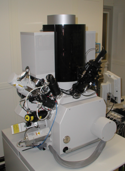
    Specifications

    • Electron Beam:
      • Resolution: 0.9 nm (15 kV)
      • Landing Voltage: 350 V - 30 kV
      • Probe current: < 22 nA
      • Maximum horizontal field width: 1.5 mm at beam coincident point
        (WD 4 mm)
    • Ion Beam:
      • Resolution: 4 nm (30 kV)
      • Landing Voltage: 500 V - 30 kV
      • Probe current: 1.5 pA - 20 nA    
      • Maximum horizontal field width: 2.5 mm at 5 kV at beam coincidence point
    • Gas injection for deposition of platinum, wolfram and SiO2
    • Etch gas supply (XeF2)
    • STEM detector

    Location

    • Microstructure laboratory

    Pulications

    Atomically flat single-crystalline gold nanostructures for plasmonic nanocircuitry
    J.-S. Huang, V. Callegari, P. Geisler, C. Brüning, J. Kern, J.C. Prangsma, X. Wu, T. Feichtner, J. Ziegler, P. Weinmann, M. Kamp, A. Forchel, P. Biagioni, U. Sennhauser, and B. Hecht
    Nature Communications 1, 150 (2010)

    Mode Imaging and Selection in Strongly Coupled Nanoantennas
    J.S. Huang, J. Kern, P. Geisler, P. Weinmann, M. Kamp, A. Forchel, P. Biagioni and B. Hecht
    Nanoletters 10, 2105 (2010)

    In-plane manipulation of quantum dots in high quality laterally contacted micropillar cavities
    J. Beetz, C. Kistner, M. Lermer, C. Schneider, S. Reitzenstein, S. Höfling, M. Kamp, and A. Forchel
    Appl. Phys. Lett. 98, 191111 (2011)

    Fe3O4/ZnO: A high-quality magnetic oxide-semiconductor heterostructure by reactive deposition
    M. Paul, D. Kufer, A. Müller, S. Brück, E. Goering, M. Kamp, J. Verbeeck, H. Tian, G. van Tendeloo, N.J.C. Ingle, M. Sing, and R. Claessen
    App. Phys. Lett. 98, 012512 (2011)